- 您现在的位置:买卖IC网 > Sheet目录1994 > DS3232MZ+ (Maxim Integrated Products)IC RTC W/SRAM I2C 8SOIC
DS3232M
±5ppm, I2C Real-Time Clock with SRAM
18
Maxim Integrated
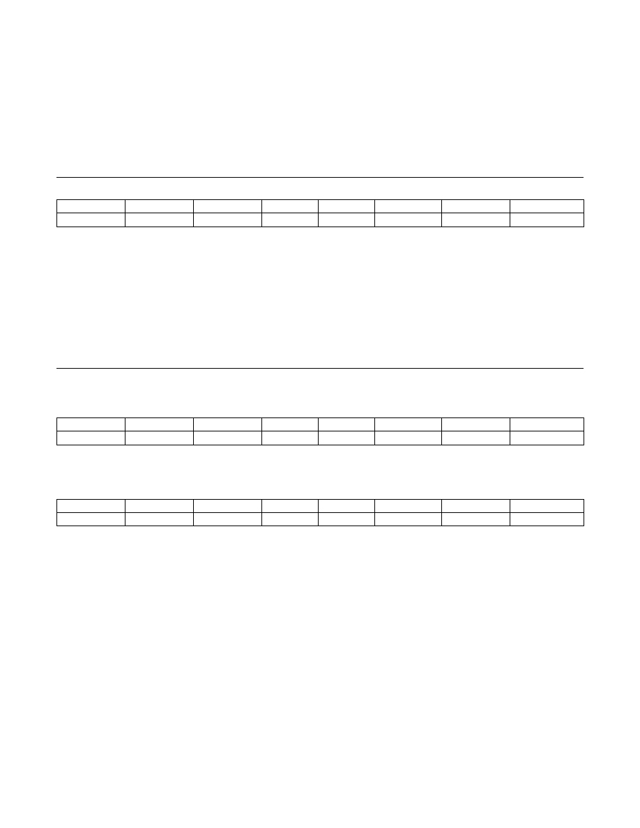
Aging Offset Register (10h)
Temperature Registers (11h–12h)
BIT 7
BIT 6
BIT 5
BIT 4
BIT 3
BIT 2
BIT 1
BIT 0
SIGN
DATA
0
The Aging Offset register takes a user-provided value to add to or subtract from the factory-trimmed value that adjusts the
accuracy of the time base. Use of the Aging Offset register is not needed to achieve the accuracy as defined in the Electrical
Characteristics tables.
The Aging Offset code is encoded in two’s complement, with bit 7 representing the SIGN bit. One LSB typically represents a
0.12ppm change in frequency. The change in ppm per LSB is the same over the operating temperature range. Positive offsets
slow the time base and negative offsets quicken the time base.
Temperature Register (Upper Byte = 11h)
BIT 7
BIT 6
BIT 5
BIT 4
BIT 3
BIT 2
BIT 1
BIT 0
SIGN
DATA
0
Temperature Register (Lower Byte = 12h)
BIT 7
BIT 6
BIT 5
BIT 4
BIT 3
BIT 2
BIT 1
BIT 0
DATA
0
Temperature is represented as a 10-bit code with a resolution of 0.25°C and is accessible at location 11h and 12h. The tem-
perature is encoded in two’s complement format. The upper 8 bits, the integer portion, are at location 11h and the lower 2 bits,
the fractional portion, are at location 12h. For example, 00011001 01b = +25.25°C. Upon power reset, the registers are set to
a default temperature of 0°C and the controller starts a temperature conversion. The temperature is read upon initial applica-
tion of VCC or I2C access on VBAT and once every second afterwards with VCC power or once every 10s with VBAT power. The
Temperature registers are also updated after each user-initiated conversion and are read only.
发布紧急采购,3分钟左右您将得到回复。
相关PDF资料
DS3232SN#T&R
IC RTC W/TCXO 20-SOIC
DS3234S#
IC RTC W/TCXO 20-SOIC
DS32C35-33#T&R
IC RTC ACCURATE I2C 3.3V 20-SOIC
DS3911T+
IC DAC 10BIT I2C QUAD 14TDFN
DS4000KI/WBGA
IC OSC TCXO 19.44MHZ 24-BGA
DS4026S+WCN
IC OSC TCXO 25MHZ 16-SOIC
DS4100HW+
IC OSC CLOCK 100MHZ 10LCCC
DS4266P+
IC OSC CLOCK 266MHZ 10-LCCC
相关代理商/技术参数
DS3232MZ+TRL
功能描述:实时时钟 RTC/TCMO/MEMS RoHS:否 制造商:Microchip Technology 功能:Clock, Calendar. Alarm RTC 总线接口:I2C 日期格式:DW:DM:M:Y 时间格式:HH:MM:SS RTC 存储容量:64 B 电源电压-最大:5.5 V 电源电压-最小:1.8 V 最大工作温度:+ 85 C 最小工作温度: 安装风格:Through Hole 封装 / 箱体:PDIP-8 封装:Tube
DS3232N
制造商:MAXIM 制造商全称:Maxim Integrated Products 功能描述:Extremely Accurate I2C RTC with Integrated Crystal and SRAM
DS3232S
制造商:Maxim Integrated Products 功能描述:Extremely Accurate I2C RTC
DS3232S-
制造商:MAXIM 制造商全称:Maxim Integrated Products 功能描述:Extremely Accurate I2C RTC with Integrated Crystal and SRAM
DS3232S#
功能描述:实时时钟 Integrated RTC/TCXO/Crystal RoHS:否 制造商:Microchip Technology 功能:Clock, Calendar. Alarm RTC 总线接口:I2C 日期格式:DW:DM:M:Y 时间格式:HH:MM:SS RTC 存储容量:64 B 电源电压-最大:5.5 V 电源电压-最小:1.8 V 最大工作温度:+ 85 C 最小工作温度: 安装风格:Through Hole 封装 / 箱体:PDIP-8 封装:Tube
DS3232S#T&R
制造商:Maxim Integrated Products 功能描述:EXTREMELY ACCURATE I2C RTC 20SOIC W - Tape and Reel 制造商:Maxim Integrated Products 功能描述:DS3232 3V 20P SOIC 制造商:Maxim Integrated Products 功能描述:IC RTC W/TCXO 20-SOIC
DS3232S#T&R
功能描述:实时时钟 Integrated RTC/TCXO/Crystal RoHS:否 制造商:Microchip Technology 功能:Clock, Calendar. Alarm RTC 总线接口:I2C 日期格式:DW:DM:M:Y 时间格式:HH:MM:SS RTC 存储容量:64 B 电源电压-最大:5.5 V 电源电压-最小:1.8 V 最大工作温度:+ 85 C 最小工作温度: 安装风格:Through Hole 封装 / 箱体:PDIP-8 封装:Tube
DS3232SN
制造商:Maxim Integrated Products 功能描述:Extremely Accurate I2C RTC